- 您现在的位置:买卖IC网 > Sheet目录510 > SI4562DY-T1-GE3 (Vishay Siliconix)MOSFET N/P-CH 20V 8-SOIC
�� �
�
�Si4562DY�
�Vishay� Siliconix�
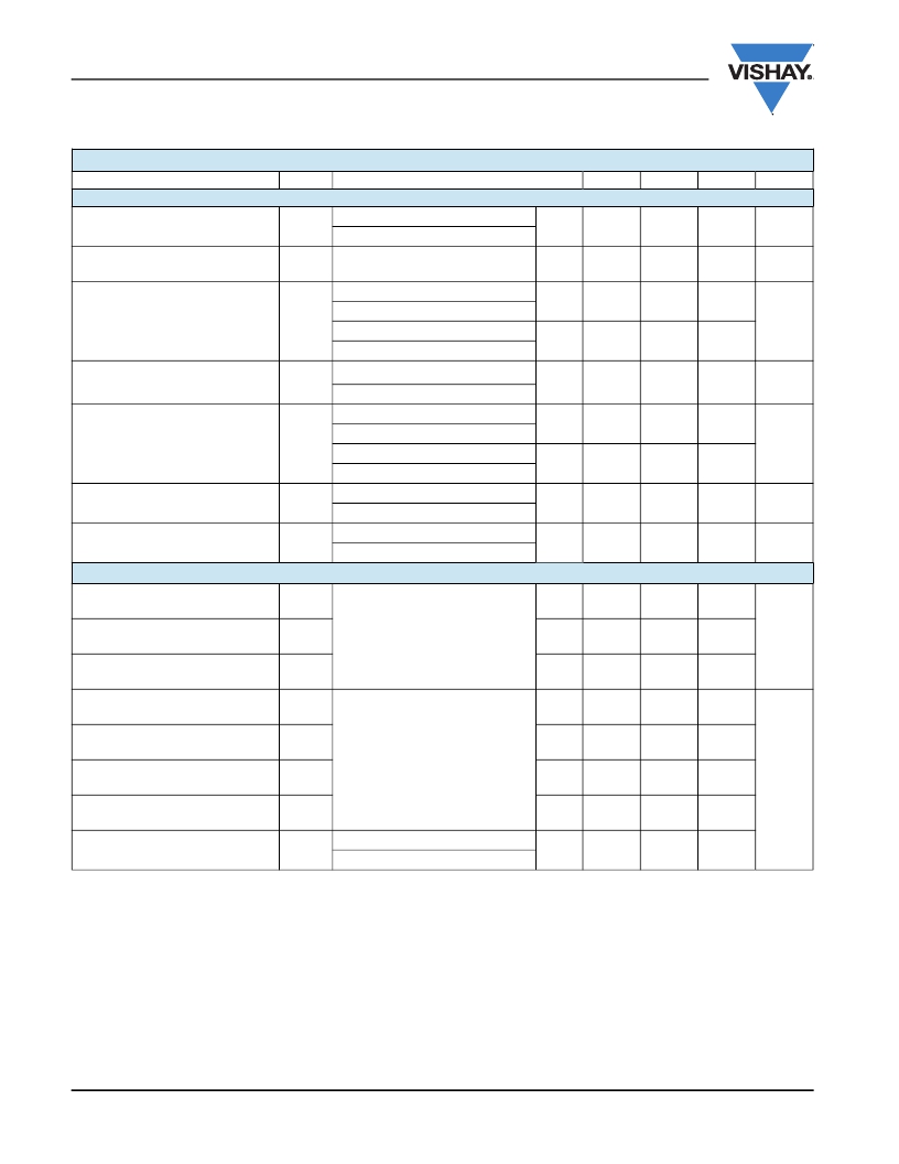
�SPECIFICATIONS� T� J� =� 25� °C,� unless� otherwise� noted�
�Parameter�
�Symbol�
�Test� Conditions�
�Min.�
�Typ.�
�Max.�
�Unit�
�Static�
�Gate� Threshold� Voltage�
�Gate-Body� Leakage�
�V� GS(th)�
�I� GSS�
�V� DS� =� V� GS� ,� I� D� =� 250� μA�
�V� DS� =� V� GS� ,� I� D� =� -� 250� μA�
�V� DS� =� 0� V,� V� GS� =� ±� 12� V�
�N-Ch�
�P-Ch�
�N-Ch�
�P-Ch�
�0.6�
�-� 0.6�
�1.6�
�-� 1.6�
�±� 100�
�±� 100�
�V�
�nA�
�V� DS� =� 20� V,� V� GS� =� 0� V�
�N-Ch�
�1�
�Zero� Gate� Voltage� Drain� Current�
�I� DSS�
�V� DS� =� -� 20� V,� V� GS� =� 0� V�
�V� DS� =� 20� V,� V� GS� =� 0� V,� T� J� =� 55� °C�
�P-Ch�
�N-Ch�
�-1�
�5�
�μA�
�V� DS� =� -� 20� V,� V� GS� =� 0� V,� T� J� =� 55� °C�
�P-Ch�
�-5�
�On-State� Drain� Current� b�
�I� D(on)�
�V� DS� ≥� 5� V,� V� GS� =� 4.5� V�
�V� DS� ≤� -� 5� V,� V� GS� =� -� 4.5� V�
�V� GS� =� 4.5� V,� I� D� =� 7.1� A�
�N-Ch�
�P-Ch�
�N-Ch�
�20�
�-� 20�
�0.019�
�0.025�
�A�
�Drain-Source� On-State� Resistance� b�
�R� DS(on)�
�V� GS� =� -� 4.5� V,� I� D� =� -� 6.2� A�
�V� GS� =� 2.5� V,� I� D� =� 6.0� A�
�P-Ch�
�N-Ch�
�0.027�
�0.025�
�0.033�
�0.035�
�Ω�
�V� GS� =� -� 2.5� V,� I� D� =� -� 5.0� A�
�P-Ch�
�0.040�
�0.050�
�Forward� Transconductance� b�
�Diode� Forward� Voltage� b�
�g� fs�
�V� SD�
�V� DS� =� 10� V,� I� D� =� 7.1� A�
�V� DS� =� -� 10� V,� I� D� =� -� 6.2� A�
�I� S� =� 1.7� A,� V� GS� =� 0� V�
�I� S� =� -� 1.7� A,� V� GS� =� 0� V�
�N-Ch�
�P-Ch�
�N-Ch�
�P-Ch�
�27�
�20�
�1.2�
�-� 1.2�
�S�
�V�
�Dynamic� b�
�Total� Gate� Charge�
�Gate-Source� Charge�
�Gate-Drain� Charge�
�Turn-On� Delay� Time�
�Rise� Time�
�Turn-Off� Delay� Time�
�Fall� Time�
�Sorce-Drain� Reverse� Recovery� Tme�
�Q� g�
�Q� gs�
�Q� gd�
�t� d(on)�
�t� r�
�t� d(off)�
�t� f�
�t� rr�
�N-Channel�
�V� DS� =� 10� V,� V� GS� =� 4.5� V,� I� D� =� 7.1� A�
�P-Channel�
�V� DS� =� -� 10� V,� V� GS� =� -� 4.5� V,� I� D� =� -� 6.2� A�
�N-Channel�
�V� DD� =� 10� V,� R� L� =� 10� Ω�
�I� D� ?� 1� A,� V� GEN� =� 4.5� V,� R� g� =� 6� Ω�
�P-Channel�
�V� DD� =� -� 10� V,� R� L� =� 10� Ω�
�I� D� ?� -� 1� A,� V� GEN� =� -� 4.5� V,� R� g� =� 6� Ω�
�I� F� =� 1.7� A,� dI/dt� =� 100� A/μs�
�I� F� =� -� 1.7� A,� dI/dt� =� 100� A/μs�
�N-Ch�
�P-Ch�
�N-Ch�
�P-Ch�
�N-Ch�
�P-Ch�
�N-Ch�
�P-Ch�
�N-Ch�
�P-Ch�
�N-Ch�
�P-Ch�
�N-Ch�
�P-Ch�
�N-Ch�
�P-Ch�
�25�
�22�
�6.5�
�7�
�4�
�3.5�
�40�
�27�
�40�
�32�
�90�
�95�
�40�
�45�
�40�
�40�
�50�
�35�
�60�
�50�
�60�
�50�
�150�
�150�
�60�
�70�
�80�
�80�
�nC�
�ns�
�Notes:�
�a.� For� design� aid� only;� not� subject� to� production� testing.�
�b.� Pulse� test;� pulse� width� ≤� 300� μs,� duty� cycle� ≤� 2� %.�
�Stresses� beyond� those� listed� under� “Absolute� Maximum� Ratings”� may� cause� permanent� damage� to� the� device.� These� are� stress� ratings� only,� and� functional� operation�
�of� the� device� at� these� or� any� other� conditions� beyond� those� indicated� in� the� operational� sections� of� the� specifications� is� not� implied.� Exposure� to� absolute� maximum�
�rating� conditions� for� extended� periods� may� affect� device� reliability.�
�www.vishay.com�
�2�
�Document� Number:� 70717�
�S09-0867-Rev.� C,� 18-May-09�
�发布紧急采购,3分钟左右您将得到回复。
相关PDF资料
SI4563DY-T1-GE3
MOSFET N/P-CH 40V 8-SOIC
SI4565ADY-T1-GE3
MOSFET N/P-CH 40V 8-SOIC
SI4567DY-T1-GE3
MOSFET N/P-CH 40V 8-SOIC
SI4622DY-T1-E3
MOSFET N-CH D-S 30V 8-SOIC
SI4632DY-T1-GE3
MOSFET N-CH 25V 8-SOIC
SI4634DY-T1-E3
MOSFET N-CH D-S 30V 8-SOIC
SI4636DY-T1-E3
MOSFET N-CH/SCHOTTKY 30V 8SOIC
SI4638DY-T1-E3
MOSFET N-CH/SCHOTTKY 30V 8SOIC
相关代理商/技术参数
SI4563DY-T1-E3
功能描述:MOSFET N-AND P-CH 40V(D-S) RoHS:否 制造商:STMicroelectronics 晶体管极性:N-Channel 汲极/源极击穿电压:650 V 闸/源击穿电压:25 V 漏极连续电流:130 A 电阻汲极/源极 RDS(导通):0.014 Ohms 配置:Single 最大工作温度: 安装风格:Through Hole 封装 / 箱体:Max247 封装:Tube
SI4563DY-T1-GE3
功能描述:MOSFET 40V 8.0A 3.25W 16/25mohm @ 10V RoHS:否 制造商:STMicroelectronics 晶体管极性:N-Channel 汲极/源极击穿电压:650 V 闸/源击穿电压:25 V 漏极连续电流:130 A 电阻汲极/源极 RDS(导通):0.014 Ohms 配置:Single 最大工作温度: 安装风格:Through Hole 封装 / 箱体:Max247 封装:Tube
SI4564DY
制造商:VISHAY 制造商全称:Vishay Siliconix 功能描述:N- and P-Channel 40 V (D-S) MOSFET
SI4564DY-T1-GE3
功能描述:MOSFET 40V 10A/9.2A N&P-CH MOSFET RoHS:否 制造商:STMicroelectronics 晶体管极性:N-Channel 汲极/源极击穿电压:650 V 闸/源击穿电压:25 V 漏极连续电流:130 A 电阻汲极/源极 RDS(导通):0.014 Ohms 配置:Single 最大工作温度: 安装风格:Through Hole 封装 / 箱体:Max247 封装:Tube
SI4565ADY-T1-E3
功能描述:MOSFET +40/-40V 6.6/9.0A RoHS:否 制造商:STMicroelectronics 晶体管极性:N-Channel 汲极/源极击穿电压:650 V 闸/源击穿电压:25 V 漏极连续电流:130 A 电阻汲极/源极 RDS(导通):0.014 Ohms 配置:Single 最大工作温度: 安装风格:Through Hole 封装 / 箱体:Max247 封装:Tube
SI4565ADY-T1-GE3
功能描述:MOSFET 40V 6.6/4.5A 3.1W 39/54mohm @ 10V RoHS:否 制造商:STMicroelectronics 晶体管极性:N-Channel 汲极/源极击穿电压:650 V 闸/源击穿电压:25 V 漏极连续电流:130 A 电阻汲极/源极 RDS(导通):0.014 Ohms 配置:Single 最大工作温度: 安装风格:Through Hole 封装 / 箱体:Max247 封装:Tube
SI4565DY
制造商:VISHAY 制造商全称:Vishay Siliconix 功能描述:N- and P-Channel 40-V (D-S) MOSFET
SI4565DY-T1-E3
制造商:Vishay Siliconix 功能描述:MOSFET N/P SO-8